
blogs.sw.siemens.com/electronic-systems-design/2023/05/16/pcb-design-best-practices-schematic-analysis
Preview meta tags from the blogs.sw.siemens.com website.
Linked Hostnames
7- 105 links toblogs.sw.siemens.com
- 1 link tocommunity.sw.siemens.com
- 1 link toeda.sw.siemens.com
- 1 link toresources.sw.siemens.com
- 1 link totwitter.com
- 1 link towww.facebook.com
- 1 link towww.linkedin.com
Thumbnail
Search Engine Appearance
https://blogs.sw.siemens.com/electronic-systems-design/2023/05/16/pcb-design-best-practices-schematic-analysis
PCB design best practices: schematic analysis - Electronic Systems Design
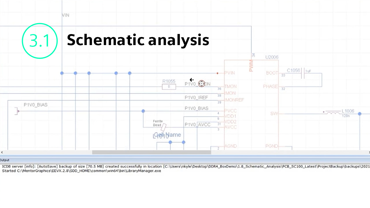
PCB schematic analysis is the automated analysis of each net within a schematic prior to pre-layout simulation and layout.
Bing
PCB design best practices: schematic analysis - Electronic Systems Design
https://blogs.sw.siemens.com/electronic-systems-design/2023/05/16/pcb-design-best-practices-schematic-analysis
PCB schematic analysis is the automated analysis of each net within a schematic prior to pre-layout simulation and layout.
DuckDuckGo
https://blogs.sw.siemens.com/electronic-systems-design/2023/05/16/pcb-design-best-practices-schematic-analysis
PCB design best practices: schematic analysis - Electronic Systems Design
PCB schematic analysis is the automated analysis of each net within a schematic prior to pre-layout simulation and layout.
General Meta Tags
16- titlePCB design best practices: schematic analysis - Electronic Systems Design
- charsetUTF-8
- viewportwidth=device-width, initial-scale=1, shrink-to-fit=no
- descriptionPCB schematic analysis is the automated analysis of each net within a schematic prior to pre-layout simulation and layout.
- robotsfollow, index, max-snippet:-1, max-video-preview:-1, max-image-preview:large
Open Graph Meta Tags
13 og:localeen_US
- og:typearticle
- og:titlePCB design best practices: schematic analysis - Electronic Systems Design
- og:descriptionPCB schematic analysis is the automated analysis of each net within a schematic prior to pre-layout simulation and layout.
- og:urlhttps://blogs.sw.siemens.com/electronic-systems-design/2023/05/16/pcb-design-best-practices-schematic-analysis/
Twitter Meta Tags
8- twitter:cardsummary_large_image
- twitter:titlePCB design best practices: schematic analysis - Electronic Systems Design
- twitter:descriptionPCB schematic analysis is the automated analysis of each net within a schematic prior to pre-layout simulation and layout.
- twitter:imagehttps://blogs.sw.siemens.com/wp-content/uploads/sites/65/2023/05/Best_practices_12_YT_1280x720.jpg
- twitter:label1Written by
Item Prop Meta Tags
3- position1
- position2
- position3
Link Tags
17- EditURIhttps://blogs.sw.siemens.com/electronic-systems-design/xmlrpc.php?rsd
- alternatehttps://blogs.sw.siemens.com/electronic-systems-design/feed/
- alternatehttps://blogs.sw.siemens.com/electronic-systems-design/comments/feed/
- alternatehttps://blogs.sw.siemens.com/electronic-systems-design/2023/05/16/pcb-design-best-practices-schematic-analysis/feed/
- alternatehttps://blogs.sw.siemens.com/electronic-systems-design/wp-json/wp/v2/posts/9580
Links
111- http://www.facebook.com/sharer/sharer.php?utm_source=facebook&utm_medium=social&utm_campaign=sw_blog_share_button&u=https://blogs.sw.siemens.com/electronic-systems-design/2023/05/16/pcb-design-best-practices-schematic-analysis
- https://blogs.sw.siemens.com
- https://blogs.sw.siemens.com/academic
- https://blogs.sw.siemens.com/additive
- https://blogs.sw.siemens.com/aerospace-defense